Impedance Matching / Signal Integrity Crash Course (Lab Edition)
 Haifei
I. Introduction
Recently, I found that many colleagues are not very familiar with impedance matching. They only know that “the impedance of (commonly used SMA/BNC) transmission lines is 50 ohms,” but do not know what this really means. The following situations often occur:
- A 50-ohm signal source connected to a scope with a 1M-ohm input:
- Huh, why did the signal become twice as large?
- A high-frequency square wave connected to a scope with a 1M-ohm input:
- Huh, why is the overshoot so severe? Is there something wrong with this signal source?
- The output signal of an MCU / DAC / FPGA connected directly, without a driver, to a 50-ohm load / 50-ohm oscilloscope input:
- Huh, why did a signal that was supposed to be 3V become only 30 mV?
All of the above result from unfamiliarity with impedance matching and transmission-line theory.
This article does not aim to derive a large number of tedious formulas. Instead, it aims to provide physical intuition for transmission lines and impedance matching. With this intuition, even if you do not remember the formulas, you can predict what phenomena will occur under what conditions and understand the causes of various strange phenomena.
Let’s begin!
II. Transmission Lines
2.1 What Is a Transmission Line?
Q: What is a transmission line?
A: A transmission line is a structure composed of two or more conductors that can support electromagnetic-wave propagation. A transmission line usually consists of two conductors: one for the signal and one for ground. Common transmission-line structures include twisted pairs, coaxial cables (commonly used SMA cables, BNC cables, etc. in laboratories), and waveguides on PCBs / chips (microstrip lines, coplanar waveguides, stripline), among others.
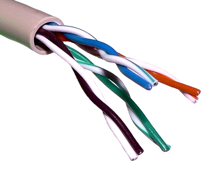
Twisted pair
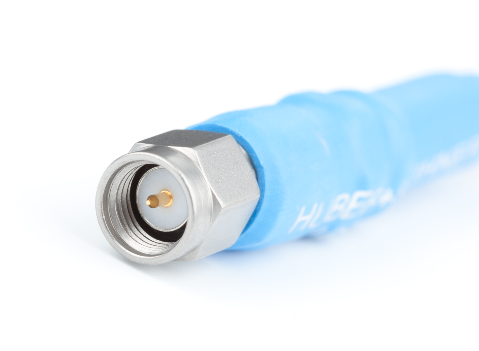
SMA connector: the center conductor carries the signal, and the outer conductor is ground
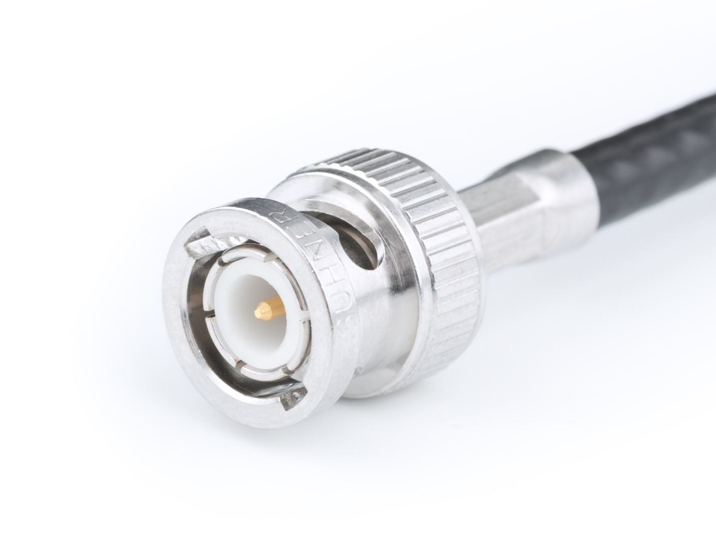
BNC connector: the center conductor carries the signal, and the outer conductor is ground
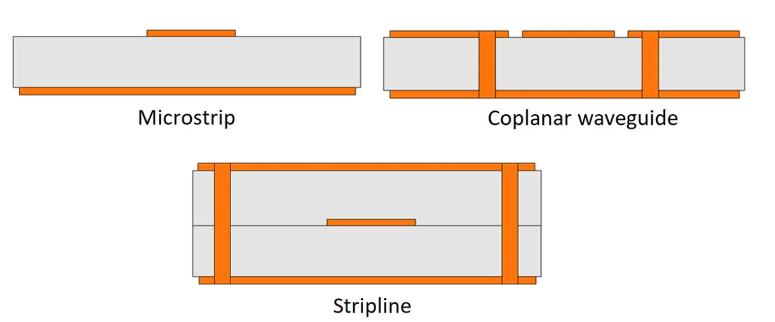
Cross-sections of microstrip, coplanar waveguide, and stripline. These structures are commonly found on high-speed PCBs. Similar structures are also present on photonic chips and superconducting quantum chips.
The advantage of coaxial cable is that its grounded outer layer naturally provides electromagnetic shielding. The same is true of stripline. Although microstrip has poorer shielding, it offers the advantages of simple design, easy fabrication, and low cost. The shielding performance of coplanar waveguide lies between the two; its advantage is more convenient impedance control.
Q: Why are transmission lines needed? Are ordinary wires not sufficient?
A: Because high-frequency signals require transmission lines for transmission.
For low-frequency signals (kHz), ordinary wires are sufficient. However, for high-frequency signals (tens of MHz to GHz), their wavelengths may be shorter than the length of the wire, so the transient behavior of the signal in the conductor must be considered. In this case, only analysis using transmission-line theory can ensure that the signal remains undistorted as much as possible.
For example, for a signal with a rise time of 0.1ns, because electromagnetic fields can propagate at most 30cm in 1ns (less in a dielectric, typically 15-20cm), the transient response in the wire must be considered as long as the wire is longer than 3cm. For such high-speed signals, even routing on a small PCB requires consideration of signal integrity, let alone long-distance transmission.
Q: Why does a transmission line require at least two wires?
A: Current must have a loop; without a loop, there is no current. If one wire carries an electrical signal, another wire is necessarily needed to provide a return path. Therefore, SMA / BNC cables consist of two conductors rather than one.
Another way to understand this is that electric field lines must have a starting point and an endpoint. Even with only one conductor, the electric field terminates at infinity or at the earth, which in practice still amounts to two conductors.
So far, these are some basic questions about transmission lines. Next, let us look at how transmission lines are modeled.
2.2 Transmission-Line Model
The following figure is commonly used to model a transmission line, where the inductance and capacitance both refer to inductance and capacitance per unit length.
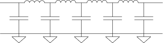
Distributed-parameter model of an ideal transmission line. The signal line has inductance per unit length, and there is capacitance per unit length between the signal line and ground line.
Why there is capacitance between the signal line and ground needs no explanation. The reason there is series inductance in the signal line is that every conductor has self-inductance: the magnetic field produced by a current opposes changes in that current (Lenz’s law).
The figure above shows an ideal transmission line without resistance. Actual transmission lines have resistance, and their dielectric is not an ideal insulator, so they are described using the model shown below:
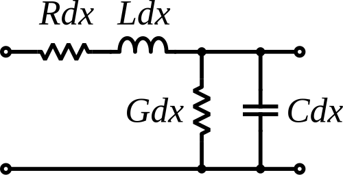
Here, \(G\) is conductance, the reciprocal of resistance.
2.3 Characteristic Impedance of a Transmission Line
The characteristic impedance of a transmission line is:
\[\begin{aligned} Z_0 = \sqrt{\frac{R+j\omega L}{G+j\omega C}} \end{aligned}\]As for how this formula is derived, one must solve partial differential equations. Interested readers may look it up themselves; it will not be discussed further here.
For an ideal transmission line, \(R=G=0\), we have
\[\begin{aligned} Z_0 = \sqrt{\frac{ L}{C}} \end{aligned}\]Note that the characteristic impedance can be complex; it just happens to be real for an ideal transmission line.
Also, note that \(Z_0\) itself is a function of \(x\):
\[\begin{aligned} Z_0(x) = \sqrt{\frac{R(x)+j\omega L(x)}{G(x)+j\omega C(x)}} \end{aligned}\]However, this function usually has a “step” shape, with discontinuities only at a few points (corresponding to where the transmission line connects to instruments in an experiment). Therefore, \(x\) is usually omitted as well.
2.4 Physical Meaning of Characteristic Impedance—Part I
The physical meaning of characteristic impedance \(Z_0\) is as follows:
A wave with angular frequency \(\omega\) propagating in a uniform transmission line (where \(Z_0\) is independent of position \(x\)) has a voltage distribution \(v(x,t)\) and current distribution \(i(x,t)\) whose ratio is \(Z_0(\omega)\).
Let the voltage be:
\(v(x,t)= A e^{-\alpha x} e^{j(\omega t - \beta x)} + B e^{\alpha x} e^{j(\omega t + \beta x)}\)
The first term is the forward-propagating signal, and the second term is the backward-propagating signal.
Then the current is:
\(i(x,t)= \frac{A}{Z_0} e^{-\alpha x} e^{j(\omega t - \beta x)} + \frac{B}{Z_0} e^{\alpha x} e^{j(\omega t + \beta x)}\)
It can be seen that \(v(x,t) = Z_0 i(x,t)\)
Note that \(Z_0\) can be complex, so voltage and current are not necessarily in phase. Of course, they are in phase for an ideal transmission line.
2.5 Physical Meaning of Characteristic Impedance—Part II
From Part I, we know that if a voltage signal \(v(t)=v_0 e^{j\omega t}\) with frequency \(\omega\) is applied to one end of an infinitely long uniform transmission line, the current entering the transmission line is \(i(t) = \frac{v_0}{Z_0(\omega)} e ^{j\omega t}\). In other words, an infinitely long uniform transmission line looks like a load \(Z_0(\omega)\) when viewed from one end.
In particular, for an ideal transmission line, \(Z_0 = \sqrt{L/C}\) is real and independent of \(\omega\), so an infinitely long ideal transmission line looks like a pure resistor when a signal arrives at one end.
Why emphasize an “infinitely long” transmission line here? Because if the transmission line is not infinitely long, then when the signal reflected from the far end returns, it will superimpose with the input signal. At that point, the relationship between input voltage and input current is no longer \(v/i=Z_0\).
III. Impedance Mismatch and Reflections
In Section II, we discussed only uniform transmission lines, i.e., transmission lines whose impedance \(Z_0\) is independent of position \(x\). Real-world situations are largely the same: whether coaxial cables (SMA/BNC) or waveguides on PCBs (Microstrip, CPW, Stripline), they are usually designed to follow \(Z_0=50\Omega\).
For differential signals, it is usually \(100\Omega\)
However, when we connect a transmission line to the receiving end of a signal, we need to consider impedance discontinuities.
For example, connect an ideal transmission line with characteristic impedance \(Z_0 = 50\Omega\) to a load \(Z \ne Z_0\).
At this point, when the signal reaches the end of the transmission line, it is reflected back. The voltage reflection coefficient is:
\[\boxed{\begin{aligned} \Gamma = \frac{Z-Z_0}{Z+Z_0} \end{aligned}}\]This formula is the core of impedance matching!
How can you remember this formula? Just remember that the numerator is the terminal load impedance \(Z\) minus the characteristic impedance \(Z_0\). This means that when \(Z \gt Z_0\), \(R\gt 0\), and the reflected signal is in phase with the incident signal. When \(Z \lt Z_0\), the reflected signal is out of phase with the incident signal. This is the commonly mentioned “half-wave loss.”
IV. Transient and Steady-State Signals
Next, we use an example to illustrate transient and steady-state signals in a transmission line.
Consider the following scenario: we have an ideal transmission line one light-year long, with characteristic impedance \(Z_0 = 50\Omega\). At the far end of the transmission line is a load \(Z = 150 \Omega \).
Now, at the near end, we connect a DC voltage source with voltage \(4\text{V}\) and output resistance \(50 \Omega\).
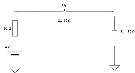
Using middle-school knowledge, we know that at steady state, the voltage across the far-end load should be \(4\text{V} \cdot \frac{150\Omega}{(150+50) \Omega} = 3\text{V}\) and the current should be \(3\text{V}/150\Omega = 20\text{mA}\).
However, in Section 2.5 we previously stated: “An infinitely long transmission line looks like a load with impedance \(Z_0\).” That is, at the instant the voltage at the near end of the transmission line rises from \(0\text{V}\) to \(4\text{V}\), the signal has no way of knowing what load is connected at the far end one light-year away—it sees only a transmission line of \(50\Omega\) in front of it.
Therefore, the voltage signal entering the transmission line is \(4\text{V} \cdot \frac{50\Omega}{(50+50) \Omega} = 2\text{V}\) and the current is \(2\text{V}/50\Omega = 40 \text{mA}\). They must travel for a year before reaching the load.
Of course, in reality it may take longer than one year, because the speed of light in a transmission line is usually lower than in vacuum; the specific speed depends on the permittivity of the dielectric. The speed of light in the most common polyethylene (PE) transmission lines is \(0.66 c\), while that in high-end Teflon (PTFE) transmission lines is \(0.8c\).
When the signal finally reaches the \(150 \Omega\) load, it is reflected back, with a reflection coefficient of:
\[\Gamma=(150-50)/(150+50)=1/2\]Therefore, the reflected signal is \(1\text{V}\). It superimposes with the incident signal \(2\text{V}\), yielding \(3\text{V}\). The excess \(20 \text{mA}\) current is reflected back as well.

The process by which the transmission line transitions from transient to steady state
When the reflected signal returns to the near end, because the output resistance of the voltage source and the transmission line satisfy the impedance-matching condition, these reflected signals are perfectly absorbed by the output resistance.
If the output resistance of the voltage source is not \(50 \Omega\), then things become troublesome: these reflected signals are reflected back again, repeatedly bouncing back and forth within the transmission line. A portion is absorbed each time, and it takes a long time before they are completely absorbed. That is, it takes a long time before the voltage across the load stabilizes at \(3 \text{V}\).
This example shows that the output resistance of the signal source should preferably match the characteristic impedance of the transmission line. In this way, even if the load is not matched, reflected signals are perfectly absorbed and do not bounce back and forth within the transmission line.
Of course, it is even better if the load is also matched to \(50 \Omega\). Then there are no reflected signals at all, and there is no interference with the voltage source. This is why, for long-distance electrical signal transmission, both the transmitter and receiver are usually matched to \(50 \Omega\).
V. Impedance Matching
Now, let us answer the questions raised at the beginning of the article one by one.
5.1 Impedance Matching Between Signal Source and Load
- A 50-ohm signal source connected to a scope with a 1M-ohm input:
- Huh, why did the signal become twice as large?
In fact, if the load is 50 ohms, it forms a voltage divider with the 50-ohm output resistance of the signal source. The voltage across the load is thus half the source voltage.
When the signal source is set to 50-ohm load mode, the voltage it displays is precisely half of its actual output voltage. That is, if you set the signal source to \(3\text{V}\), it actually outputs \(6 \text{V}\), so the load receives exactly \(3\text{V}\), the same as the displayed value.
At this point, if you change the load to \(1 \text{M}\Omega\), it receives all of \(6 \text{V}\). This is why the signal doubles.
Likewise, if the signal source is set to high-impedance load mode, it displays whatever voltage the voltage source outputs. At this point, if you connect a \(50\Omega\) load, the voltage across the load is only half the displayed voltage.
Why have both 50-ohm and 1M-ohm (high-impedance) modes? This is because when a signal must be transmitted over a long distance, both the signal source and the load must be matched to the impedance of the transmission line, namely \(50\Omega\), to prevent reflection-induced distortion. When the transmission distance is very short (the transmission-line length is much smaller than the signal rise time), impedance matching is unnecessary. In that case, switching to high-impedance mode saves power and reduces heating.
5.2 High-Frequency Signals
- A high-frequency square wave connected to a scope with a 1M-ohm input:
- Huh, why is the overshoot so severe? Is there something wrong with this signal source?
Square waves contain a great many high-frequency components. The key factor here is not the frequency of the square wave, but the width of its rising edge.
Even if the frequency of your square wave is not high, impedance matching must be considered if the width of its rising edge is shorter than the length of the transmission line.
Without impedance matching, overshoot will be observed near the rising/falling edges. This is the manifestation of signal reflections caused by impedance mismatch.
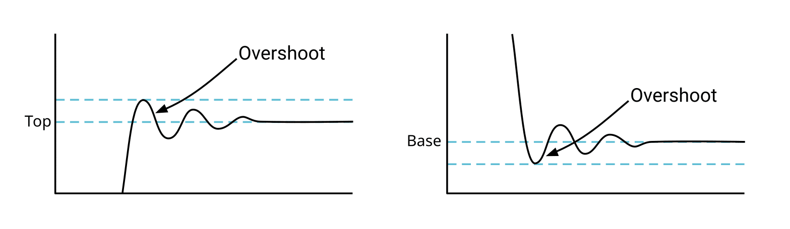
Overshoot
If only the receiving end lacks impedance matching, that is still manageable: the signal reflected back to the transmitting end will be absorbed. But if the transmitting end is not impedance-matched either, the signal will bounce back and forth in the transmission line, corresponding to the multiple ripples in the overshoot waveform.
5.3 Drivers
- The output signal of an MCU / DAC / FPGA connected directly, without a driver, to a 50-ohm load / 50-ohm oscilloscope input:
- Huh, why did a signal that was supposed to be 3V become only 30 mV?
For commonly used TTL / CMOS33 logic-level standards, the voltage is 5V or 3.3V. To drive a 50-ohm load, the required current is:
\[3.3\text{V} / 50\Omega = 66 \text{mA}\]That is, to drive a 50-ohm load at \(3.3\text{V}\), the maximum output current must be at least \(66 \text{mA}\). For \(5\text{V}\), it is \(100\text{mA}\).
However, for chips such as microcontrollers / DACs / FPGAs, the output current of their pins is usually not very large, with a maximum of only a dozen or so mA. This means that they cannot drive a 50-ohm load. If forced to do so, a signal that should have been \(3.3\text{V}\) may become less than \(1\text{V}\).
What should be done in this case? Connect a buffer / voltage follower / driver to the pin, then drive the load from its output. Their output logic levels are the same as their inputs, but they can drive 50-ohm loads and improve signal quality.
Personally, my favorite is the ISL55110 dual-channel high-speed driver; its input/output logic levels can be defined independently. It is much more convenient than building a follower with an operational amplifier.
VI. An Introduction to Signal Integrity
In addition to impedance matching, signal integrity includes many other topics, including:
- Parasitic-inductance-related topics
- Return paths
- Placement of vias and decoupling capacitors
- Crosstalk
- Loss-related topics
- Conductor loss
- Dielectric loss
- Surface roughness
- Skin effect (which causes greater loss in high-frequency signals)
- Timing-related topics
- Differential-pair length matching
- Clock jitter
- Eye-diagram analysis
- Power integrity
- Decoupling, resonance, ground bounce
- ESD
However, these topics are usually matters that PCB designers need to consider. In most cases, users only need to understand impedance matching.
If there is an opportunity in the future, this channel will also introduce some signal-integrity issues that need to be considered in PCB design. Stay tuned~