High-Precision Time Measurement—Analysis of TDC / Time Tagger Principles and Architecture
 Haifei
1. What Is a TDC / Time Tagger?
A Time-to-Digital Converter (TDC) is essentially an extremely precise timer (at the picosecond level) that assigns a high-precision timestamp (Timestamp) to every input pulse signal.
Therefore, a TDC is also called a Time Tagger, where “Tag” means assigning a timestamp.
TDCs / Time Taggers are central to experiments such as Hong-Ou-Mandel interference and fluorescence lifetime measurements; it can be said that quantum optics experiments can hardly do without them.
2. TDC Architecture
The overall architecture of a TDC is very simple, as shown below:
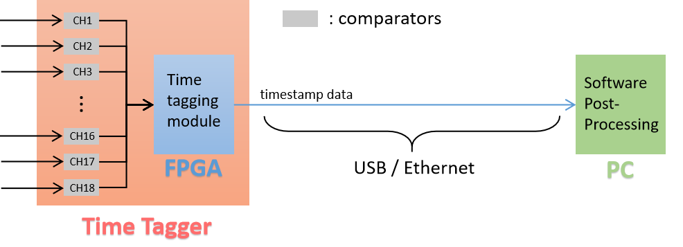
Architecture of a TDC / Time Tagger. Image source: created by the author
Each channel of a TDC is connected to a comparator. The comparator converts the input analog pulse signal into a digital pulse signal. The FPGA assigns high-precision timestamps to these digital pulses and transfers them to the host computer for post-processing via protocols such as USB / Ethernet.
Of course, if the chip-design capability is strong enough, the FPGA can also be replaced with a custom ASIC (application-specific integrated circuit).
Taking the Swabian Instruments Time Tagger as an example, its internal design consists of a core board (carrying the FPGA) + a baseboard (carrying the comparators). The advantage of this design is that it is easy to test and highly scalable.
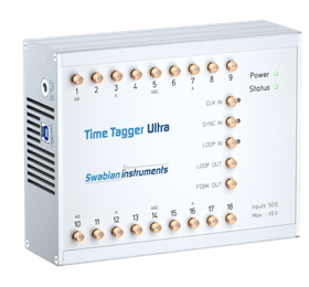
Swabian Instruments Time Tagger. Image source: https://www.swabianinstruments.com/time-tagger/
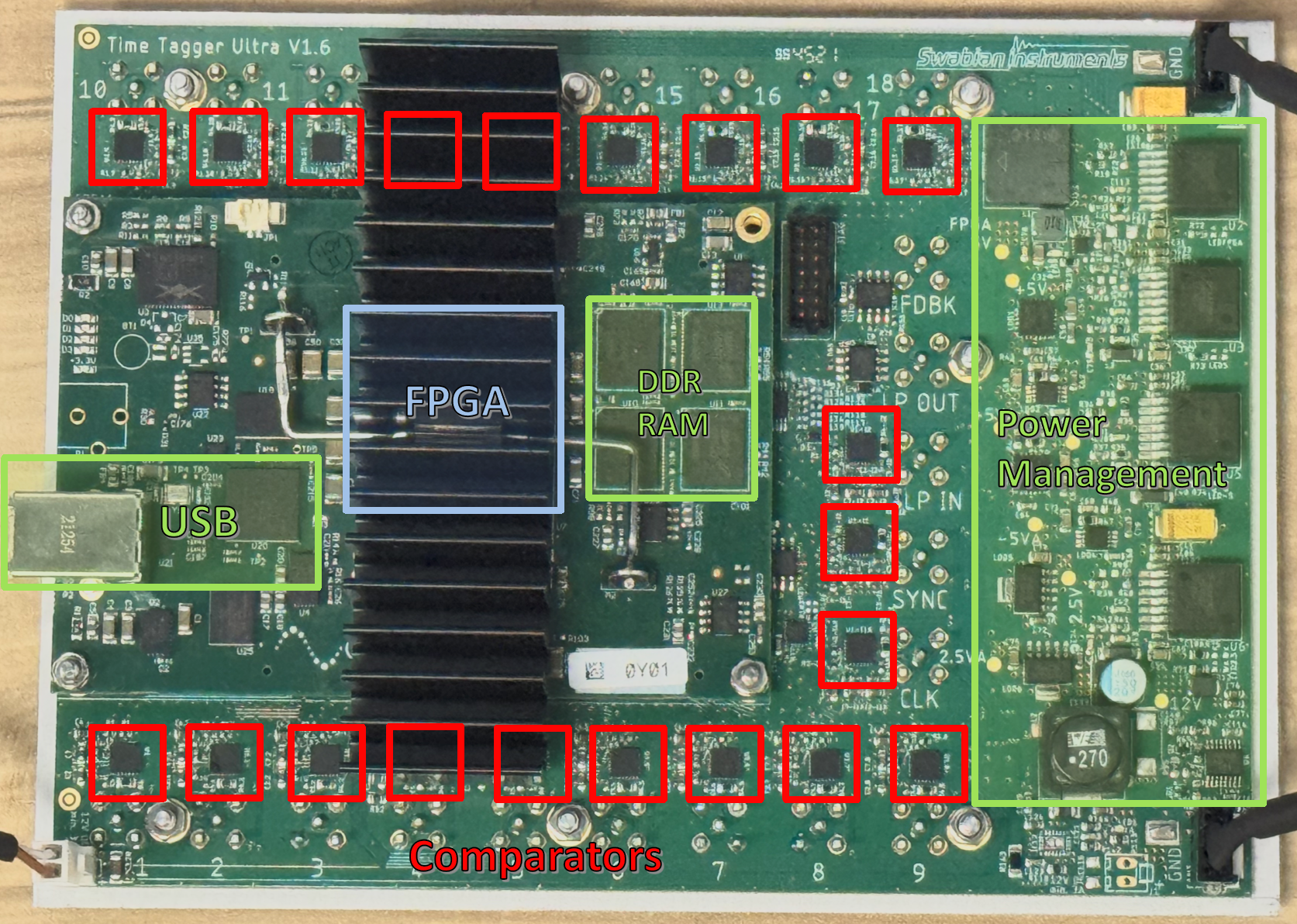
Structural analysis of the Swabian Instruments Time Tagger. Image source: created by the author.
The FPGA used in this Swabian Instruments Time Tagger Ultra is from the Xilinx Kintex 7 series (xc7k160t), which is considered a mid-to-low-end series (28 nm process). It costs around USD 400–500.
The comparator is the Texas Instruments LMH7322, compatible with the LVDS standard and featuring RMS random jitter of 500–600 fs. It costs around USD 10.
Adding clock management, DDR, USB, and various other chips, my personal estimate is that—even at the absolute maximum—the BOM material cost of the entire board would not exceed USD 2,000.
Yet Swabian Instruments can sell this complete unit for EUR 20,000! How?
The answer is intellectual property: primarily the on-chip FPGA hardware design, and secondarily the comprehensive host-side software and API.
In the next section, we will introduce the on-chip FPGA hardware design.
3. Principles of Implementing a TDC with an FPGA
Those familiar with FPGAs know that their clock frequency can only reach a few hundred MHz at most. Beyond that, timing violations usually occur. However, the timestamps assigned by a TDC have ps-level precision, corresponding to frequencies of several hundred GHz! So how exactly does an FPGA implement a TDC? It cannot possibly run at several hundred GHz, can it?
In fact, the FPGA implementation of a TDC is highly ingenious. The core component used is the carry logic (CARRY) needed during addition.
The carry logic in the Xilinx 7 series is CARRY4, while that in the Xilinx Ultrascale series is CARRY8. As their names imply, the former has 4 bits and the latter has 8 bits. Below, we use CARRY4 as an example.
The block diagram of the CARRY4 primitive is as follows:
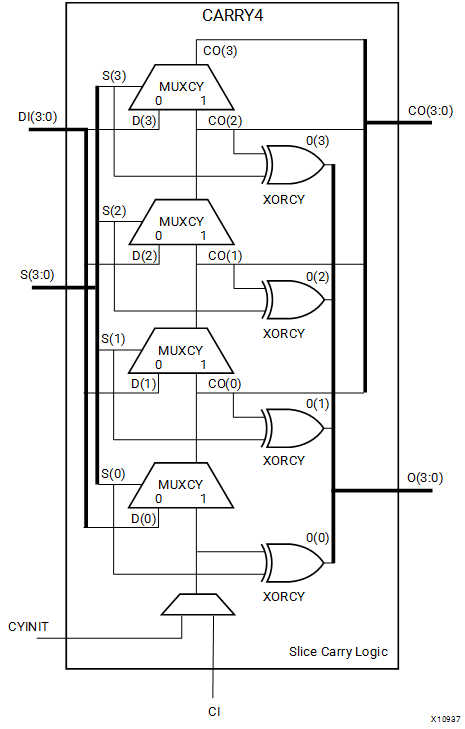
Image source: https://docs.amd.com/r/en-US/ug953-vivado-7series-libraries/CARRY4
Does it look complicated? Do not worry; it will be explained below.
In Verilog, it can be instantiated through the CARRY4 primitive:
| |
Before introducing the principles by which it implements a TDC, let us first discuss its primary function—calculating carries in addition.
3.1 Full Adders
Let us first review how combinational logic circuits perform addition.
The circuit responsible for addition is called a full adder. An n-bit full adder consists of cascaded 1-bit full adders.
A 1-bit full adder has three input signals: two addends (A, B) and a carry input (CI). It has two output signals: the sum (O) and the carry output (CO).
Below is the truth table for a 1-bit full adder:
| A | B | CI | CO | O |
|---|---|---|---|---|
| 0 | 0 | 0 | 0 | 0 |
| 1 | 0 | 0 | 0 | 1 |
| 0 | 1 | 0 | 0 | 1 |
| 1 | 1 | 0 | 1 | 0 |
| 0 | 0 | 1 | 0 | 1 |
| 1 | 0 | 1 | 1 | 0 |
| 0 | 1 | 1 | 1 | 0 |
| 1 | 1 | 1 | 1 | 1 |
We can write the logical expressions as follows:
\[\begin{aligned} \text{O} &= \text{A} \oplus \text{B} \oplus \text{CI} \\ \text{CO} &= \text{A} \cdot \text{B} + \text{A} \cdot \text{CI} + \text{B} \cdot \text{CI} \end{aligned}\]Here, the symbol \(\oplus\) represents exclusive OR (XOR), the symbol \(\cdot\) represents AND, and the symbol \(+\) represents OR. AND has higher precedence than OR.
With \(1\)-bit full adders, we only need to connect the \(\text{CO}\) of the \((n-1)\)th bit to the \(\text{CI}\) of the \(n\)th bit to implement an \(n\)-bit full adder.
In this way, we can use XOR gates, AND gates, and OR gates to perform addition.
However, the above logical expressions can be further simplified, thereby reducing the number of logic gates. Let \(\text{DI}=\text{A}\cdot \text{B}\) and \(\text{S}=\text{A} \oplus \text{B}\). Then
\[\begin{aligned} \text{O} &= \text{A} \oplus \text{B} \oplus \text{CI} \\ &= \text{S}\oplus \text{CI} \\ \text{CO} &= \text{A} \cdot \text{B} + \text{A} \cdot \text{CI} + \text{B} \cdot \text{CI}\\ &= \text{A}\cdot \text{B} + (\text{A} \oplus \text{B})\cdot \text{CI} \\ &= (\text{A} \oplus \text{B}) \,? \,\text{CI} : (\text{A}\cdot \text{B})\\ &= \text{S} \, ? \, \text{CI}: \text{DI} \end{aligned}\]Here, \(a \,?\, b:c\) is a ternary operator, meaning \(\text{if }a,\text{ then }b,\text{ else }c\). This operation is implemented by a MUX (multiplexer).
DI is called the generator, while S is called the propagator. As the names imply, DI generates carries and S propagates carries.
Now, we vectorize the above logical expressions:
\[\begin{aligned} \text{O}[n]&=\text{S}[n] \oplus \text{DI}[n] \\ \text{CO}[n]&= \text{S}[n]\,?\, \text{CO}[n-1] : \text{DI}[n] \end{aligned}\]We can then draw the circuit diagram (using a 4-bit full adder as an example):
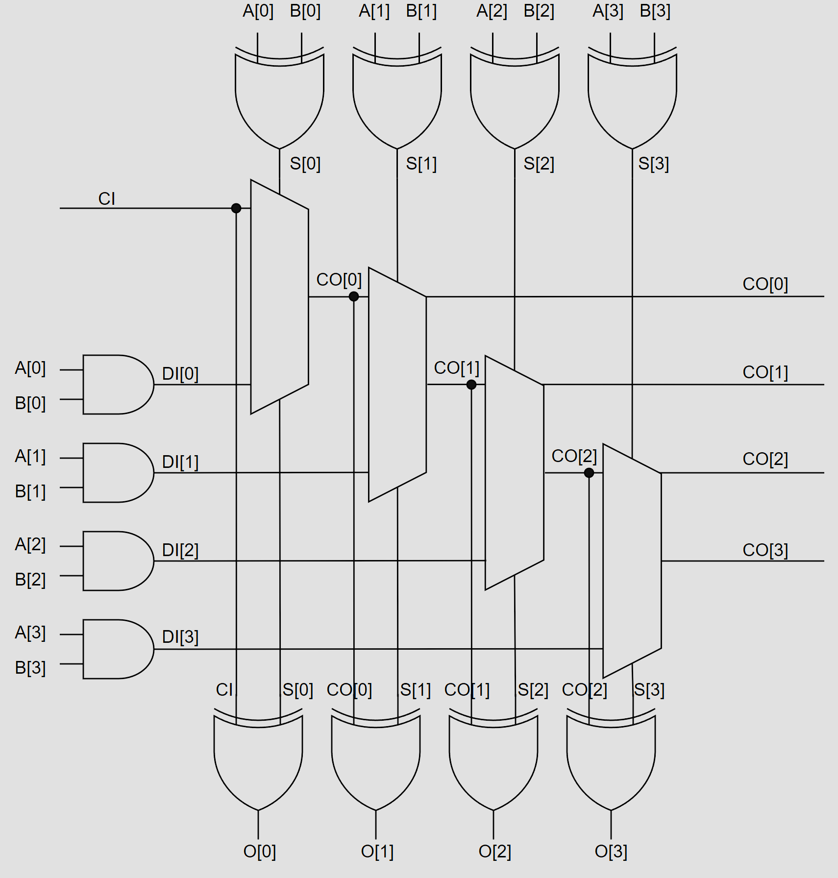
Circuit diagram of a 4-bit full adder. Image source: created by the author
This circuit implements the operation \(\{\text{CO}, \,\text{O[3:0]}\} = \text{A[3:0]} + \text{B[3:0]} + \text{CI}\).
3.2 Structure of CARRY4
If we extract the core portion of the circuit diagram from the previous section, we obtain CARRY4:
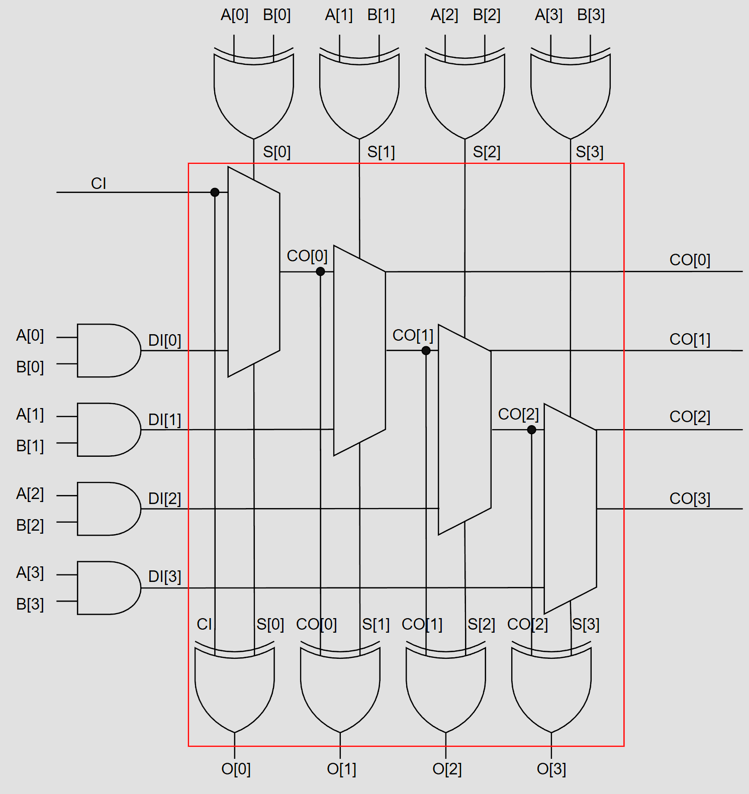
The portion enclosed by the red box is CARRY4. Image source: created by the author
Let us compare it with the circuit diagram in the official documentation:
Image source: https://docs.amd.com/r/en-US/ug953-vivado-7series-libraries/CARRY4
Are they exactly the same?
The only difference is that CI can be overridden by CYINIT. When CYINIT is 1, it outputs 1; when CYINIT is 0, it outputs CI. This is merely for programming convenience.
For example, when calculating subtraction, the logical expression is \(\text{O} = \text{A} + \sim\text{B} + 1\), where \(\sim\) denotes bit-wise NOT. Therefore, when performing subtraction, it is only necessary to set CYINIT of the CARRY4 at the least significant bit to 1.
3.3 CARRY4 as a High-Precision Delay Line
In the previous two sections, we introduced the primary function of CARRY4—performing addition. Now, let us introduce its role in a TDC—a picosecond-level delay line.
There is a relatively long critical path in CARRY4:
\[\text{CI} \rightarrow \text{CO}[0] \rightarrow \text{CO}[1] \rightarrow \text{CO}[2] \rightarrow \text{CO}[3] \]The computation of any combinational logic gate requires picosecond-level time. Specifically, in the path above, each arrow takes from a few picoseconds to several tens of picoseconds.
If we connect multiple CARRY4 units end to end, we obtain a very long delay line with picosecond-level delay resolution:
\[\text{CI} \rightarrow \text{CO}[0] \rightarrow \text{CO}[1] \rightarrow \text{CO}[2] \rightarrow \cdots \rightarrow \text{CO}[N-1]\]As can be seen from logical expression \(\text{CO}[n]= \text{S}[n]\,?\, \text{CO}[n-1] : \text{DI}[n] \), as long as we set all \(\text{S}[n]\) to logic high, the carry signal can propagate along this chain. The logic level of \(\text{DI}[n]\) does not matter and does not affect propagation of the carry signal.
This actually simulates how humans propagate carries when performing addition: imagine calculating \(1111_2 + 0001_2 = 10000_2\). We first calculate the least significant digit \(1+1=10\) and find that it generates a carry, so we record it in the next digit. This causes the next digit to generate a carry as well, and so on. The time required for a computer to calculate each of these carries is from a few to several tens of picoseconds.
As shown below, we connect the input pulse (trigger signal) to \(\text{CI}\) and record \(\text{CO}[N-1:0]\) at the rising edge of the next clock cycle, allowing us to determine the time interval \(\tau\) shown in the figure. This makes it possible to determine the arrival time of the input pulse with picosecond precision.
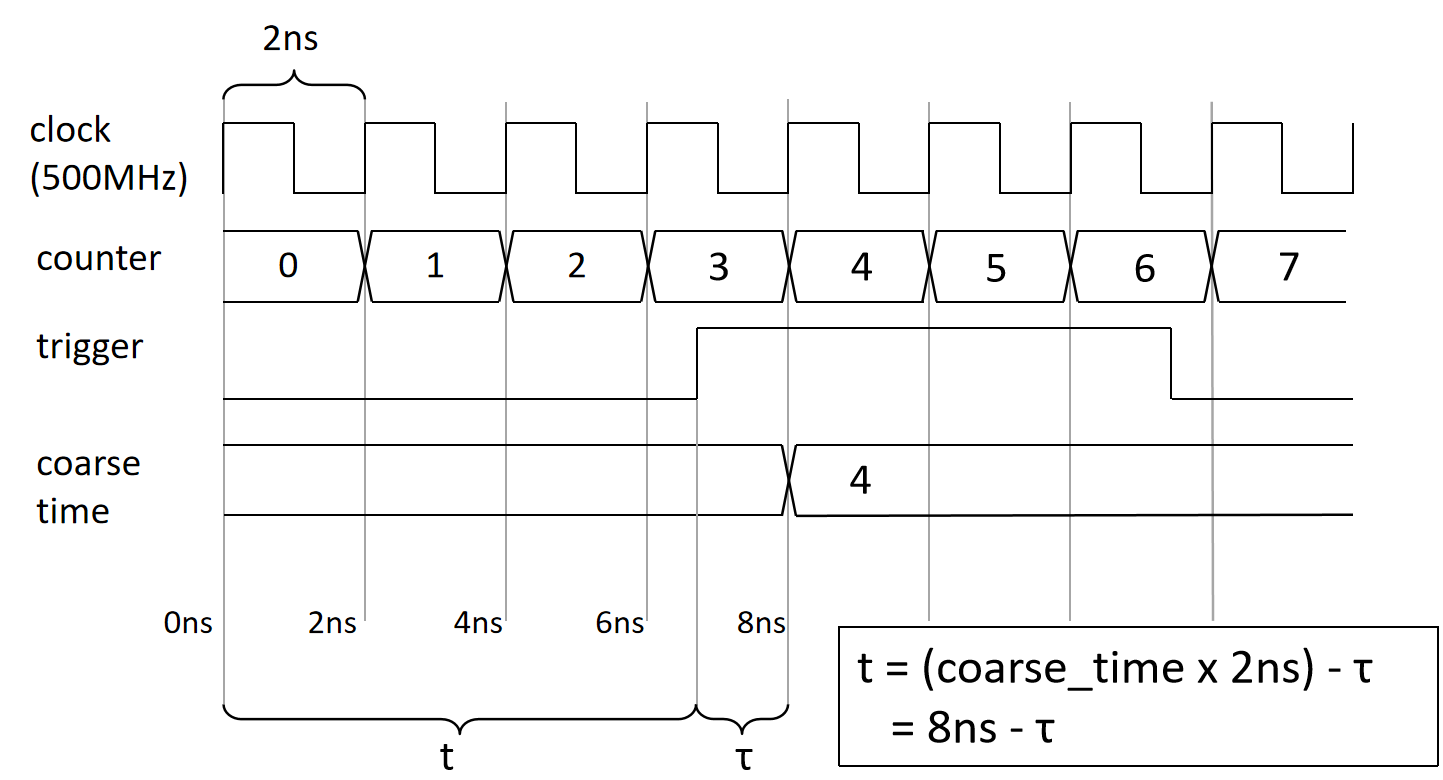
TDC timing diagram. Image source: created by the author
Some readers have probably spotted the issue: according to this operating principle, if two pulses arrive within one clock period, would it not be possible to record only one of them (for example, the first one)? That is correct. This is why TDCs / Time Taggers also have dead time, typically from several to more than ten nanoseconds, determined by the FPGA clock frequency.
Of course, if a dedicated ASIC can be designed with a custom delay line, its performance will certainly be better than that of an FPGA. After all, CARRY4 / CARRY8 in FPGAs were not originally intended to serve as delay lines.
4. Summary
This article introduced the architecture and operating principles of FPGA-based TDCs (Time-to-Digital Converters) / Time Taggers. Among these, the high-precision delay lines constructed using CARRY4/CARRY8 form a key part of the FPGA hardware design.
References
[1] Castelvero, L., López Grande, I. H. & Pruneri, V. High-Performance Time-to-Digital Conversion on a 16-nm Ultrascale+ FPGA. IEEE Access 12, 149569–149579 (2024).
[2] Zhu, M., Qi, X., Cui, T. & Gao, Q. Tapped delay line for compact time-to-digital converter on UltraScale FPGA and its coding method. Nuclear Instruments and Methods in Physics Research Section A: Accelerators, Spectrometers, Detectors and Associated Equipment 1056, 168639 (2023).
[3] Hua, Y. & Chitnis, D. A Highly Linear and Flexible FPGA-Based Time-to-Digital Converter. IEEE Trans. Ind. Electron. 69, 13744–13753 (2022).